
In the ever-evolving landscape of semiconductor manufacturing, precision and reliability are paramount. Enter test wafer solutions, the unsung heroes of the semiconductor industry. These unassuming, circular pieces of silicon play a critical role in ensuring the quality and functionality of microchips and electronic components that power our modern world.
Test wafers are indispensable tools that enable semiconductor manufacturers to fine-tune their production processes, diagnose issues, and enhance the yield of their semiconductor devices. In this comprehensive guide, we’ll dive deep into the world of test wafer solutions, exploring their various types, purposes, manufacturing processes, materials, designs, testing methods, quality control measures, applications across industries, and the exciting future trends shaping their evolution.
Types of Test Wafers
Before delving into the intricacies of test wafer solutions, let’s start with the basics. Test wafers come in several flavors, each tailored to specific needs. The most common types include monitor, dummy, defect, and the lesser-known but equally crucial short-loop wafers. Monitor substrates are used to assess the overall health of the semiconductor fabrication process. Dummy wafers mimic real ones but lack actual chip structures and serve as placeholders in the production line.
Defect ones, on the other hand, intentionally contain known defects, helping manufacturers detect and address issues early on. These Short Loop Wafers play a vital role in certain specialized testing scenarios, providing unique insights into semiconductor performance.
Purpose of Test Wafers
The purpose of test wafers in semiconductor manufacturing is paramount. These specialized wafers act as surrogate guinea pigs, allowing engineers to meticulously fine-tune production processes. Test substrates enable the assessment of critical parameters like film thickness, etch rates, and pattern uniformity. By mimicking the characteristics of production wafers, they serve as a controlled environment where deviations from desired specifications can be detected and rectified.
Ultimately, the goal is to enhance the yield and quality of semiconductor devices. This plays a crucial role in diagnosing issues, optimizing equipment, and ensuring that the end products meet the stringent standards of the semiconductor industry. Without them, achieving the precision and reliability required in semiconductor manufacturing would be a formidable challenge.
Manufacturing Process
The journey begins with the same raw material as production substrates: silicon. The manufacturing process involves a series of steps, including wafer slicing, lithography, and etching. First, a silicon ingot is sliced into thin substrates. These substrates are then coated with various materials and patterns using lithography. Etching is subsequently employed to create structures, such as transistors and interconnects. The result is a test substrate with distinct structures and patterns.
Test Wafer Materials

While silicon is the most common material for examination wafers, other materials like gallium arsenide and silicon carbide are used for specific applications. The choice of material depends on the intended use and the properties required. For instance, gallium arsenide is favored for its superior performance in high-frequency applications, making it a go-to choice for RF (radio frequency) semiconductor testing.
Test Wafer Design
Designing them is a meticulous process that involves careful consideration of the structures and patterns to be etched onto the substrate’s surface. These patterns mimic the actual components found in production substrates, enabling precise examination and evaluation. Engineers must strike a balance between complexity and simplicity, as overly intricate designs can lead to longer times and higher costs.
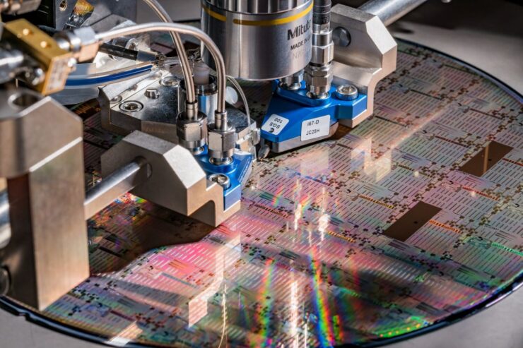
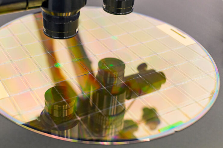
Testing Methods
Testing methods for wafers are diverse and precise, tailored to reveal specific insights into semiconductor quality. Electrical assess crucial parameters like conductivity, while scanning electron microscopy (SEM) visualizes surface defects. X-ray inspection delves into internal structures, while optical inspection and focused ion beam (FIB) techniques aid in various analyses.
These methods collectively ensure comprehensive evaluation, offering manufacturers an array of tools to fine-tune processes and enhance semiconductor yields. In a rapidly evolving industry, the ability to employ these advanced techniques is paramount, allowing manufacturers to stay at the forefront of semiconductor technology and meet the ever-increasing demands for smaller, faster, and more efficient electronic devices.
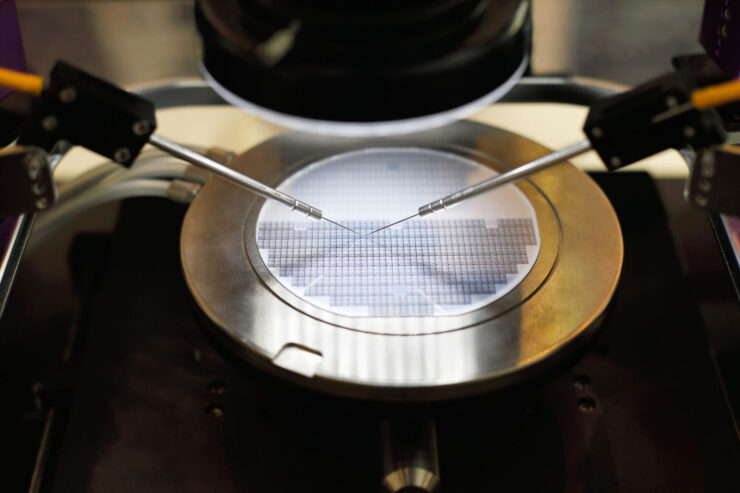
Quality Control
Ensuring reliability is essential to guarantee accurate results. Rigorous quality control measures are implemented throughout the manufacturing process. This includes periodic inspections to verify substrate integrity, as well as stringent calibration and maintenance of equipment. Any deviation from the desired specifications is thoroughly investigated and corrected to maintain the accuracy of examination substrate results.
Applications
The applications span a multitude of industries, underscoring their critical role in modern technology. In aerospace, they ensure the reliability of avionics and navigation systems. Telecommunications companies rely on them to guarantee the performance of network components. In the automotive sector, test substrates are instrumental in enhancing the efficiency and safety of vehicles.
Moreover, the consumer electronics industry depends on these wafers to deliver cutting-edge smartphones, tablets, and gadgets to consumers. From medical devices to renewable energy systems, test substrates are the unseen champions that uphold quality and innovation across diverse sectors. Their adaptability and precision make them indispensable in an increasingly interconnected world, where technology’s reliability is paramount.
Future Trends
As technology continues to advance at a rapid pace, so too do the demands placed on test wafer solutions. Emerging trends in semiconductor manufacturing, such as nanotechnology, 3D integration, and quantum computing, present new challenges and opportunities. Test substrate solutions will need to evolve to meet these demands, requiring innovative approaches, materials, and design. Miniaturization and automation will likely play key roles in the future of test substrate manufacturing.
Conclusion
In conclusion, test wafer solutions are the unsung heroes of the semiconductor industry, silently ensuring the reliability and performance of the electronic devices that have become integral to our daily lives. From their various types and essential roles in manufacturing to the meticulous fabrication process, materials, and rigorous methods, these unassuming substrates are the linchpin of quality control in semiconductor production.
With industries ranging from aerospace to consumer electronics relying on semiconductor devices, the importance of examination substrates cannot be overstated. As technology advances, so too will the demands on these vital tools, propelling them into a future filled with exciting opportunities and challenges.
In the ever-evolving world of semiconductors, one thing remains constant: the crucial role in shaping the technology that powers our modern world.